3 Computer Architecture
To write lower level code, a programmer must understand the architecture of a computer. It is similar to when one writes programs in a software framework, he must know what kinds of problems the framework solves, and how to use the framework by its provided software interfaces. But before getting to the definition of what computer architecture is, we must understand what exactly is a computer, as many people still think that a computer is a regular computer we put on a desk, or at best, a server. Computers come in various shapes and sizes, and some are devices that people never imagine are computers, let alone that code can run on them.
3.1 What is a computer?
A computer is a hardware device that consists of at least a processor (CPU), a memory device and input/output interfaces. All the computers can be grouped into two types:
- Single-purpose computer
-
is a computer built at the hardware level for specific tasks. For example, dedicated application encoders/decoders, timers, image/video/sound processors.
- General-purpose computer
-
is a computer that can be programmed (without modifying its hardware) to emulate various features of single-purpose computers.
3.1.1 Server
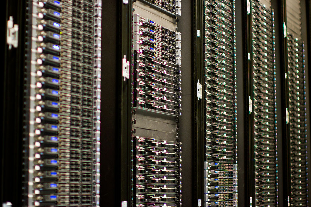
A server is a general-purpose high-performance computer with huge resources to provide large-scale services for a broad audience. The audience are people with their personal computer connected to a server.
3.1.2 Desktop Computer
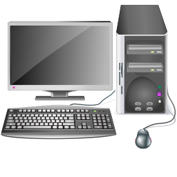
A desktop computer is a general-purpose computer with an input and output system designed for a human user, with moderate resources enough for regular use. The input system usually includes a mouse and a keyboard, while the output system usually consists of a monitor that can display a large amount of pixels. The computer is enclosed in a chassis large enough for putting various computer components such as a processor, a motherboard, a power supply, a hard drive, etc.
3.1.3 Mobile Computer
A mobile computer is similar to a desktop computer with fewer resources but can be carried around.

A laptop

A tablet

A mobile phone
Mobile computers
3.1.4 Game Consoles
Game consoles are similar to desktop computers but are optimized for gaming. Instead of a keyboard and a mouse, the input system of a game console consists of game controllers, which are devices with a few buttons for controlling on-screen objects; the output system is a television. The chassis is similar to a desktop computer but is smaller. Game consoles use custom processors and graphic processors but are similar to ones in desktop computers. For example, the first Xbox used a custom Intel Pentium III processor.
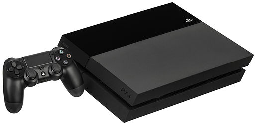
A PlayStation 4
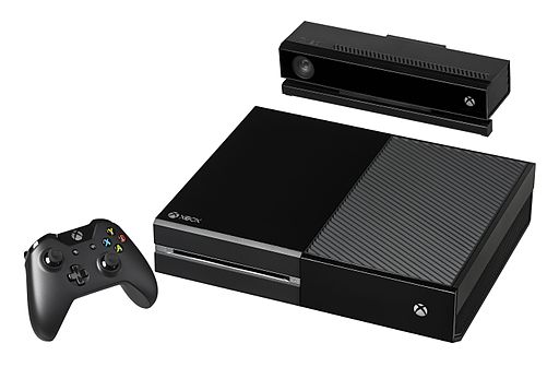
An Xbox One
Game consoles of the eighth generation (2013)
Handheld game consoles are similar to game consoles, but incorporate both the input and output systems along with the computer in a single package.
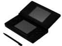
A Nintendo DS
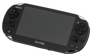
A PS Vita
Some Handheld Consoles
3.1.5 Embedded Computer
An embedded computer is a single-board or single-chip computer with limited resources designed for integrating into larger hardware devices.
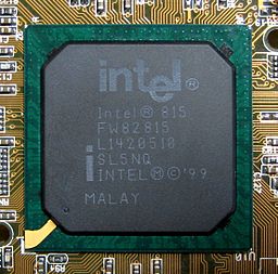
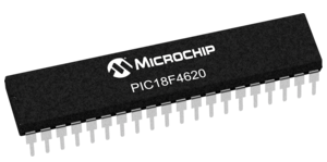
A microcontroller is an embedded computer designed for controlling other hardware devices. A microcontroller is mounted on a chip. Microcontrollers are general-purpose computers, but with limited resources so that it is only able to perform one or a few specialized tasks. These computers are used for a single purpose, but they are still general-purpose since it is possible to program them to perform different tasks, depending on the requirements, without changing the underlying hardware.
Another type of embedded computer is system-on-chip. A system-on-chip is a full computer on a single chip. Though a microcontroller is housed on a chip, its purpose is different: to control some hardware. A microcontroller is usually simpler and more limited in hardware resources as it specializes only in one purpose when running, whereas a system-on-chip is a general-purpose computer that can serve multiple purposes. A system-on-chip can run like a regular desktop computer that is capable of loading an operating system and run various applications. A system-on-chip is typically found in a smartphone, such as the Apple A5 SoC used in the iPad 2 and iPhone 4S (2011), or the Qualcomm Snapdragon used in many Android phones.

Be it a microcontroller or a system-on-chip, there must be an environment where these devices can connect to other devices. This environment is a circuit board called a PCB - Printed Circuit Board. A printed circuit board is a physical board that contains lines and pads to enable electron flows between electrical and electronics components. Without a PCB, devices cannot be combined to create a larger device. As long as these devices are hidden inside a larger device and contribute to a larger device that operates at a higher level layer for a higher level purpose, they are embedded devices. Writing a program for an embedded device is therefore called embedded programming. Embedded computers are used in automatically controlled devices including power tools, toys, implantable medical devices, office machines, engine control systems, appliances, remote controls and other types of embedded systems.
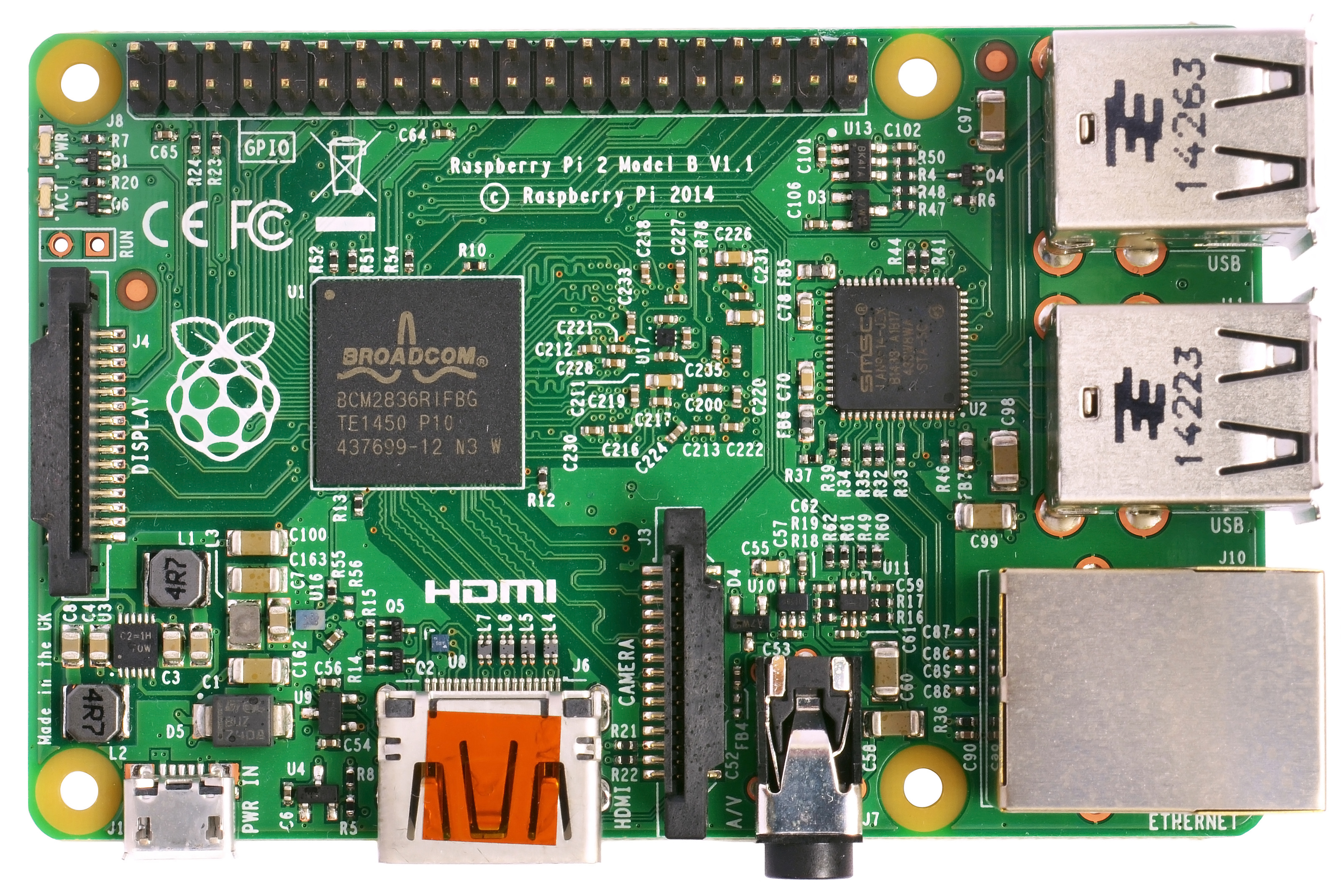
Physical View
Raspberry Pi 2 Model B (2015), a single-board computer built around a Broadcom system-on-chip (the large chip in the middle); the smaller chip on the right is the USB and Ethernet controller.
The line between a microcontroller and a system-on-chip is blurry. As hardware keeps getting more powerful, a microcontroller can get enough resources to run a minimal operating system on it for multiple specialized purposes. In contrast, a system-on-chip is powerful enough to handle the job of a microcontroller. However, using a system-on-chip as a microcontroller would not be a wise choice as the price will rise significantly, and we also waste hardware resources since the software written for a microcontroller requires little computing resources.
3.1.6 Field Programmable Gate Array
Field Programmable Gate Array (FPGA) is a hardware array of reconfigurable gates that makes circuit structure programmable after it is shipped away from the factory1. Recall that in the previous chapter, each 74HC00 chip can be configured as a gate, and a more sophisticated device can be built by combining multiple 74HC00 chips. In a similar manner, each FPGA device contains thousands of chips called logic blocks, which are more complicated than a 74HC00 chip and can be configured to implement a Boolean logic function. These logic blocks can be chained together to create a high-level hardware feature. This high-level feature is usually a dedicated algorithm that needs high-speed processing.
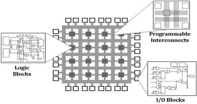
Digital devices can be designed by combining logic gates, without regarding actual circuit components, since the physical circuits are just multiples of CMOS circuits. Digital hardware, including various components in a computer, is designed by writing code, like a regular programmer, by using a language to describe how gates are wired together. This language is called a Hardware Description Language. Later the hardware description is compiled to a description of connected electronic components called a netlist, which is a more detailed description of how gates are connected.
The difference between FPGA and other embedded computers is that programs in FPGA are implemented at the digital logic level, while programs in embedded computers like microcontrollers or system-on-chip devices are implemented at assembly code level. An algorithm written for a FPGA device is a description of the algorithm in logic gates, which the FPGA device then follows to configure itself to run the algorithm. An algorithm written for a microcontroller is in assembly instructions that a processor can understand and act accordingly.
FPGA is applied in the cases where the specialized operations are unsuitable and costly to run on a regular computer such as real-time medical image processing, cruise control system, circuit prototyping, video encoding/decoding, etc. These applications require high-speed processing that is not achievable with a regular processor because a processor wastes a significant amount of time in executing many non-specialized instructions - which might add up to thousands of instructions or more - to implement a specialized operation, thus more circuits at physical level to carry the same operation. An FPGA device carries no such overhead; instead, it runs a single specialized operation implemented in hardware directly.
3.1.7 Application-Specific Integrated Circuit
An Application-Specific Integrated Circuit (or ASIC) is a chip designed for a particular purpose rather than for general-purpose use. ASIC does not contain a generic array of logic blocks that can be reconfigured to adapt to any operation like an FPGA; instead, every logic block in an ASIC is made and optimized for the circuit itself. FPGA can be considered as the prototyping stage of an ASIC, and ASIC as the final stage of circuit production. ASIC is even more specialized than FPGA, so it can achieve even higher performance. However, ASICs are very costly to manufacture and once the circuits are made, if design errors happen, everything is thrown away, unlike the FPGA devices which can simply be reprogrammed because of the generic gate array.
3.2 Computer Architecture
The previous section examined various classes of computers. Regardless of shapes and sizes, every computer is designed from an architecture, from high level to low level.
At the highest-level is the Instruction Set Architecture.
At the middle-level is the Computer Organization.
At the lowest-level is the Hardware.
3.2.1 Instruction Set Architecture
An instruction set is the basic set of commands and instructions that a microprocessor understands and can carry out.
An Instruction Set Architecture, or ISA, is the design of an environment that implements an instruction set. Essentially, a runtime environment similar to those interpreters of high-level languages. The design includes all the instructions, registers, interrupts, memory models (how memory is arranged to be used by programs), addressing modes, I/O, etc., of a CPU. The more features (e.g. more instructions) a CPU has, the more circuits are required to implement it.
3.2.2 Computer organization
Computer organization is the functional view of the design of a computer. In this view, hardware components of a computer are presented as boxes with input and output that connect to each other and form the design of a computer. Two computers may have the same ISA, but different organizations. For example, both AMD and Intel processors implement x86 ISA, but the hardware components of each processor that make up the environments for the ISA are not the same.
Computer organizations may vary depending on a manufacturer’s design, but they all originate from the Von Neumann architecture[^8]:
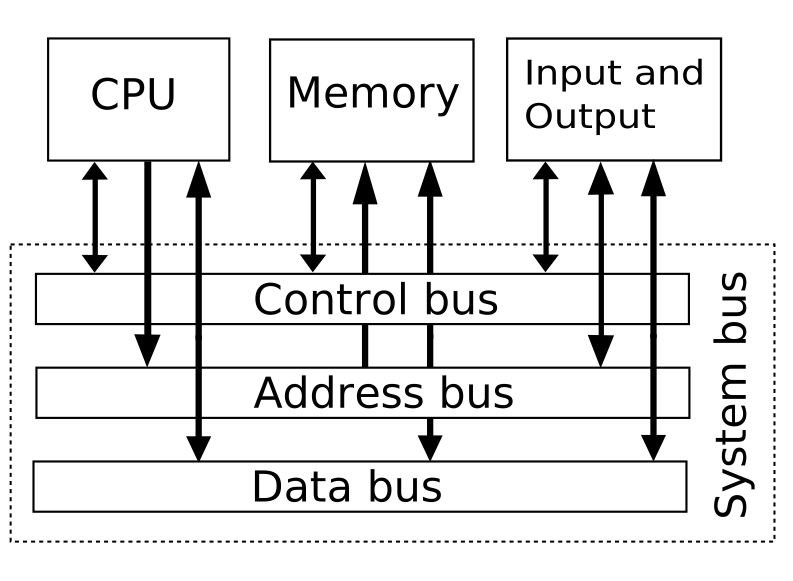
Von-Neumann Architecture
- CPU
-
fetches instructions continuously from main memory and executes them.
- Memory
-
stores program code and data.
- Bus
-
is a set of electrical wires for sending raw bits between the above components.
- I/O Devices
-
are devices that give input to a computer i.e. keyboard, mouse, sensor, etc, or take the output from a computer i.e. monitor takes information sent from CPU to display it, LED turns on/off according to a pattern computed by CPU, etc.
The Von-Neumann computer operates by storing its instructions in main memory, and CPU repeatedly fetches those instructions into its internal storage for executing, one after another. Data are transferred through a data bus between CPU, memory and I/O devices, and where to store in the devices is transferred through the address bus by the CPU. This architecture completely implements the fetch decode execute cycle.
The earlier computers were just the exact implementations of the Von Neumann architecture, with CPU, memory and I/O devices communicating through the same bus. Today, a computer has more buses, each specialized in a type of traffic. However, at the core, they are still the Von Neumann architecture. To write an OS for a Von Neumann computer, a programmer needs to be able to understand and write code that controls the core components: CPU, memory, I/O devices, and bus.
CPU, or Central Processing Unit, is the heart and brain of any computer system. Understanding a CPU is essential to writing an OS from scratch:
To use these devices, a programmer needs to control the CPU to use the programming interfaces of other devices. The CPU is the only way, as the CPU is the only device a programmer can use directly and the only device that understands code written by a programmer.
In a CPU, many OS concepts are already implemented directly in hardware, e.g. task switching, paging. A kernel programmer needs to know how to use the hardware features, to avoid duplicating such concepts in software, thus wasting computer resources.
CPU built-in OS features boost both OS performance and developer productivity because those features are actual hardware, the lowest possible level, and developers are free to implement such features.
To effectively use the CPU, a programmer needs to understand the documentation provided by the CPU manufacturer. For example, the Intel® 64 and IA-32 Architectures Software Developer’s Manual, which Intel publishes free of charge on its website. This book cites it as “Intel SDM”, by volume, chapter and section number, and the numbers are those of the September 2026 edition (revision 093). Intel inserts chapters between editions, so if your copy is older or newer and a number does not match, search for the section title instead; the chapters on segmentation (Volume 3A, chapters 2 and 3) and the basic execution environment (Volume 1, chapter 3) have kept their numbers for years, the later chapters of Volume 3A have not.
After understanding one CPU architecture well, it is easier to learn other CPU architectures.
A CPU is an implementation of an ISA, effectively the implementation of an assembly language (and depending on the CPU architecture, the language may vary). Assembly language is one of the interfaces that are provided for software engineers to control a CPU, thus control a computer. But how can every computer device be controlled with only access to the CPU? The simple answer is that a CPU can communicate with other devices through these two interfaces, thus commanding them:
- Registers
-
are a hardware component for high-speed data access and communication with other hardware devices. Registers allow software to control hardware directly by writing to registers of a device, or receive information from a hardware device when reading from registers of a device.
Not all registers are used for communication with other devices. In a CPU, most registers are used as high-speed storage for temporary data. Other devices that a CPU can communicate with always have a set of registers for interfacing with the CPU.
- Port
-
is a specialized register in a hardware device used for communication with other devices. When data is written to a port, it causes a hardware device to perform some operation according to values written to the port. The difference between a port and a register is that a port does not store data, but delegates data to some other circuit.
These two interfaces are extremely important, as they are the only interfaces for controlling hardware with software. Writing device drivers is essentially learning the functionality of each register and how to use them properly to control the device.
Memory is a storage device that stores information. Memory consists of many cells. Each cell is a byte with its address number, so a CPU can use such address number to access an exact location in memory. Memory is where software instructions (in the form of machine language) are stored and retrieved to be executed by CPU; memory also stores data needed by some software. Memory in a Von Neumann machine does not distinguish between which bytes are data and which bytes are software instructions. It’s up to the software to decide. If somehow data bytes are fetched, the CPU will execute them if such bytes represent valid instructions, but will produce undesirable results. To a CPU, there’s no code and data; both are merely different types of data for it to act on: one tells it how to do something in a specific manner, and one is necessary materials for it to carry such action.
The RAM is controlled by a device called a memory controller. Since 2008, Intel processors have this device embedded, so the CPU has a dedicated memory bus connecting the processor to the RAM. On older CPUs2, however, this device was located in a chip also known as MCH or Memory Controller Hub. In this case, the CPU does not communicate directly to the RAM, but to the MCH chip, and this chip then accesses the memory to read or write data. The first option provides better performance since there is no middleman in the communications between the CPU and the memory.
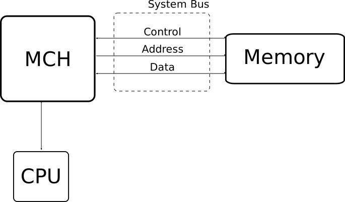
CPU with an external memory controller (before 2008)
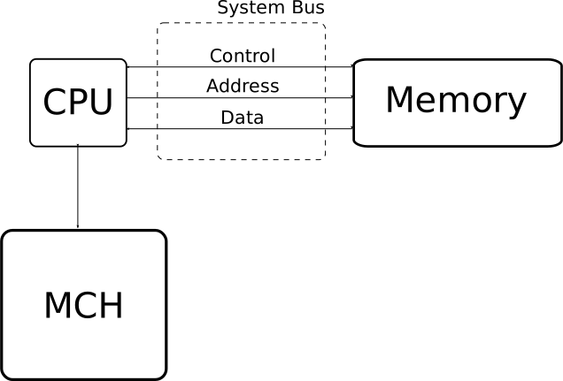
CPU with an integrated memory controller (since 2008)
CPU - Memory Communication
At the physical level, RAM is implemented as a grid of cells that each contain a transistor and an electrical device called a capacitor, which stores charge for short periods of time. The transistor controls access to the capacitor; when switched on, it allows a small charge to be read from or written to the capacitor. The charge on the capacitor slowly dissipates, requiring the inclusion of a refresh circuit to periodically read values from the cells and write them back after amplification from an external power source.
Bus is a subsystem that transfers data between computer components or between computers. Physically, buses are just electrical wires that connect all components together and each wire transfers a single bit of data. The total number of wires is called bus width, and is dependent on how many wires a CPU can support. If a CPU can only accept 16 bits at a time, then the bus has 16 wires connecting from a component to the CPU, which means the CPU can only retrieve 16 bits of data a time.
3.2.3 Hardware
Hardware is a specific implementation of a computer. A line of processors implement the same instruction set architecture and use nearly identical organizations but differ in hardware implementation. For example, the Core i7 family provides a model for desktop computers that is more powerful but consumes more energy, while another model for laptops is less performant but more energy efficient. To write software for a hardware device, we seldom need to understand a hardware implementation if documents are available. Computer organization and especially the instruction set architecture are more relevant to an operating system programmer. For that reason, the next chapter is devoted to studying the x86 instruction set architecture in depth.
3.3 x86 architecture
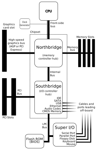
A chipset is a chip with multiple functions. Historically, a chipset is actually a set of individual chips, and each is responsible for a function, e.g. memory controller, graphic controllers, network controller, power controller, etc. As hardware progressed, the set of chips were incorporated into a single chip, thus more space, energy, and cost efficient. In a desktop computer, various hardware devices are connected to each other through a PCB called a motherboard. Each CPU needs a compatible motherboard that can host it. Each motherboard is defined by its chipset model, which determines the environment that a CPU can control. This environment typically consists of
a slot or more for CPU
a chipset of two chips which are the Northbridge and Southbridge chips
Northbridge chip is responsible for the high-performance communication between CPU, main memory and the graphics card.
Southbridge chip is responsible for the communication with I/O devices and other devices that are not performance sensitive.
slots for memory sticks
a slot or more for graphics cards.
generic slots for other devices, e.g. network card, sound card.
ports for I/O devices, e.g. keyboard, mouse, USB.
To write a complete operating system, a programmer needs to understand how to program these devices. After all, an operating system manages hardware automatically to free application programs from doing so. However, of all the components, learning to program the CPU is the most important, as it is the component present in any computer, regardless of what type a computer is. For this reason, the primary focus of this book will be on how to program an x86 CPU. Even when solely focused on this device, a reasonably good minimal operating system can be written. The reason is that not all computers include all the devices as in a normal desktop computer. For example, an embedded computer might only have a CPU and limited internal memory, with pins for getting input and producing an output; yet, operating systems were written for such devices.
However, learning how to program an x86 CPU is a daunting task, with 3 primary manuals written for it: almost 500 pages for volume 1, over 2000 pages for volume 2 and over 1000 pages for volume 3. It is an impressive feat for a programmer to master every aspect of x86 CPU programming. Fortunately, an operating system only needs a small part of it, and the section on the x86 execution environment at the end of this chapter tells which part.
3.4 Two vendors, one architecture
The previous section spoke of the x86 manual, and the rest of this book cites Intel. It is time to say precisely what x86 is, because two companies define it, and a reader who owns an AMD processor, or who downloads AMD’s manual, should know what changes. Almost nothing does, and this section explains why.
Intel designed the 32-bit architecture, which it calls
IA-32, and has documented it since the 80386. AMD, which had
built compatible processors since the 1980s, extended it to 64 bits in
2003 under the name AMD64: 64-bit registers and eight more of
them, a 64-bit address space, and a new operating mode that AMD named
long mode. Intel adopted the extension the following year,
first under the name EM64T and today as Intel 64, and called
the mode IA-32e mode. So “long mode” and “IA-32e mode” are two
names for the same thing. Linux, gcc and QEMU use the AMD names (the
architecture is x86_64 or amd64, and the flag
that says a CPU supports it is lm), the Intel manual uses
its own, and this book says “long mode” in prose and “IA-32e” when it
quotes Intel. The architecture every PC has run since is therefore a
joint work: a 32-bit core defined by Intel, a 64-bit extension defined
by AMD, and both vendors implementing both.
Both vendors publish a complete manual, free of charge. AMD’s is the AMD64 Architecture Programmer’s Manual (APM), in five volumes (AMD 2026): Volume 1, Application Programming (publication 24592); Volume 2, System Programming (24593); Volume 3, General-Purpose and System Instructions (24594); Volume 4, 128-bit and 256-bit Media Instructions (26568); Volume 5, 64-bit Media and x87 Floating-Point Instructions (26569). Search AMD’s website for the publication number. The counterpart of Intel SDM Volume 3A, the volume this book cites most, is APM Volume 2, and the section numbers below are those of its revision 3.45 (July 2026).
For everything in this book the two manuals describe the same hardware, and the code runs unchanged on both: real-address mode and protected mode, segment descriptors, the GDT and the IDT, the exception vectors, page tables, the APIC, the I/O ports of the chipset and the switch to long mode. We cite Intel because the first edition did, and because the Intel manual is organized in a way that is easier to navigate on a first reading: one chapter per mechanism, with the figure of each data structure where the mechanism is explained. APM Volume 2 covers the same ground with the same figures, in a different order and with different names. Its chapter 1, “System-Programming Overview”, is the counterpart of SDM Volume 3A chapter 2, and its figure 1-6, “Operating Modes of the AMD64 Architecture”, in section 1.3, is the counterpart of Intel’s figure 2-3. AMD groups real mode, protected mode and virtual-8086 mode under the name legacy mode (section 1.3.4), as opposed to long mode (section 1.3.1). Chapter 4 of the APM, “Segmented Virtual Memory”, corresponds to chapter 3 of the SDM; chapter 5, “Page Translation and Protection”, to chapter 5; chapter 8, “Exceptions and Interrupts”, to chapter 7; and chapter 14, “Processor Initialization and Long Mode Activation”, to chapter 12 and to our appendix C. Appendix D, Reading the Intel and AMD manuals, says more about how each is organized. Reading one mechanism in both manuals is the best way to separate what the architecture requires from what one author chose to say first, and exercise 3.3 asks you to try.
Where the vendors differ, the book says so when it gets there. The differences that matter to a kernel are few:
The fast system-call instructions. AMD introduced
syscallandsysret; Intel introducedsysenterandsysexit. Both vendors now implement both pairs, but not in every mode: AMD supportssysenterin legacy mode only (APM Volume 2, sections 6.1.1 and 6.1.2), and Intel supportssyscallin 64-bit mode only. 64-bit kernels usesyscall, which both support there; the kernel of chapter 13 uses theintinstruction, which works everywhere.Some model-specific registers (MSRs) and some leaves of the
cpuidinstruction exist on one vendor only. The ones this book uses,EFERand the basiccpuidleaves, are common to both (APM Volume 2, section 3.1.7, “Extended Feature Enable Register (EFER)”, and section 3.3, “Processor Feature Identification”).The virtualization extensions are entirely different designs: Intel’s VT-x, in SDM Volume 3C, and AMD’s AMD-V, which the manual calls Secure Virtual Machine (APM Volume 2, chapter 15). This book uses neither; QEMU uses whichever your host has.
Cache sizes, performance counters, machine-check registers and power management belong to the organization and the hardware, not to the ISA, and differ between models of the same vendor as well.
How does software find out which vendor it runs on? With the
cpuid instruction, leaf 0, which returns a twelve-character
string in ebx, edx and ecx:
GenuineIntel or AuthenticAMD. Chapter 10
prints it from our kernel. Under QEMU you will see the string of
whichever CPU model you asked for, which is why a book written on an
Intel machine can be checked, listing by listing, on an AMD one.
3.5 Intel Q35 Chipset
Q35 is an Intel chipset released in September 2007. Q35 is used as an example of a high-level computer organization because later we will use QEMU to emulate a Q35 system, which is the most recent Intel chipset that QEMU emulates. Though released in 2007, Q35 remains a faithful model of how a PC is organized, and the knowledge can still be reused for current chipset models. With a Q35 chipset, the emulated CPU is also modern enough to use the latest software manuals from Intel.
What changed since 2007 is mostly where the functions live, not what they are. Starting with the Nehalem microarchitecture (2008), the memory controller moved into the CPU package, and the graphics controller followed a few years later; the Northbridge therefore disappeared, and the Southbridge was renamed the Platform Controller Hub (PCH). A current motherboard thus has a single chipset chip, connected to the CPU by a dedicated link, where Q35 has two. The software view, however, is the same: devices are still discovered and configured through PCI configuration space, the legacy devices (the interrupt controller, the timer, the keyboard controller, the serial port) still answer at the same I/O port addresses, and the firmware still describes the machine through ACPI tables. This is why what you learn on Q35 applies to the computer on your desk.
Figure 3.1 is the classic motherboard organization that Q35 follows, with the Northbridge and the Southbridge as two separate chips.
3.6 x86 Execution Environment
An execution environment is an environment that provides the facility to make code executable. The execution environment needs to address the following question:
Supported operations? data transfer, arithmetic, control, floating-point, etc.
Where are operands stored? registers, memory, stack, accumulator
How many explicit operands are there for each instruction? 0, 1, 2, or 3
How is the operand location specified? register, immediate, indirect, etc.
What type and size of operands are supported? byte, int, float, double, string, vector, etc.
etc.
Chapter 3 of Intel SDM Volume 1, “Basic Execution Environment”, answers these questions for x86 in about forty pages, and you should read it in full before chapter 4; nothing in this book replaces it. What follows is a reading guide: the parts of that environment that the rest of this book relies on, with the exact sections of the manual where each is described, so that you know what to look for and what to skip on a first reading.
3.6.1 Operating modes
An x86 CPU does not have a single execution environment but three, called operating modes, and the environment changes with the mode. They are described in Intel SDM Volume 3A, section 2.2, “Modes of Operation”, and the transitions between them are summarized in figure 2-3 of the same chapter:
- Real-address mode
-
is the mode of the original 8086, and the mode the CPU is in after power-on or reset. Registers are 16 bits wide, the address space is 1 MB, and there is no memory protection: any code can read, write or execute any address. The BIOS runs in this mode, and so does the bootloader of chapter 7, because the BIOS hands control to it in this mode.
- Protected mode
-
is the native mode of the 32-bit CPU. Registers are 32 bits wide, the address space is 4 GB, and the CPU enforces memory protection through segmentation and, optionally, paging. The kernel of this book runs in this mode from chapter 9 on. Protected mode contains a sub-mode, virtual-8086 mode, to run real-mode programs under a protected-mode operating system; we will not use it.
- IA-32e mode
-
also called long mode, is the 64-bit mode, which has two sub-modes: 64-bit mode for 64-bit programs and compatibility mode to run 32-bit programs under a 64-bit operating system. The CPU can only enter it from protected mode, with paging enabled; this is why a 64-bit kernel goes through the same steps as ours, and one more. Chapter 15 describes that last step.
A fourth mode, system management mode, is entered by the firmware for power management and is invisible to the operating system; the manual mentions it, and we can forget it.
3.6.2 General-purpose registers
Intel SDM Volume 1, section 3.4.1, “General-Purpose
Registers”, lists eight 32-bit registers: eax,
ebx, ecx, edx, esi,
edi, ebp and esp. Each can hold
an address or an integer and most instructions accept any of them, but
the instruction set gives each a conventional role, and some
instructions use a specific register implicitly; the table in that
section lists the roles, and you will recognize them in the output of
objdump from chapter 4 on:
eaxis the accumulator: the result of a function is returned in it, and multiplication, division and I/O instructions use it implicitly.ecxis the counter for loops and for the repeated string instructions.edxholds the high half of a 64-bit product or dividend, and the port number of theinandoutinstructions that talk to devices in chapter 10.esiandediare the source and destination pointers of the string instructions.espis the stack pointer:push,pop,callandretread and write it, and the CPU itself pushes onto the stack it points to when an interrupt arrives (chapter 11).ebpis the base pointer of the current stack frame; chapter 4 shows how a compiled C function uses it to find its arguments and local variables.ebxhas no fixed role in 32-bit mode.
The low 16 bits of each register are accessible under the names of
the 8086, ax, bx, cx,
dx, si, di, bp,
sp, and the two halves of ax to
dx under the names ah/al to
dh/dl (figure 3-5 of the section). In
real-address mode only these 16-bit names are available, which is why
the bootloader of chapter 7 is written with them.
3.6.3 The instruction pointer and EFLAGS
The instruction pointer eip holds the address
of the next instruction. It cannot be read or written directly; it
changes through the control-transfer instructions jmp,
call, ret, through interrupts, and the
call instruction saves it on the stack. Intel SDM Volume 1,
section 3.5, “Instruction Pointer”.
The eflags register is a set of single-bit
flags (Intel SDM Volume 1, section 3.4.3, “EFLAGS
Register”, with figure 3-8 giving the bit positions). The ones to
know are:
The status flags CF (carry, bit 0), ZF (zero, bit 6), SF (sign, bit 7) and OF (overflow, bit 11). Arithmetic and comparison instructions set them to describe their result, and the conditional jumps test them:
jejumps if ZF is set,jbif CF is set,jlif SF differs from OF, and so on. Everyifand every loop of a C program becomes acmpthat sets these flags followed by a jump that reads them, as chapter 4 shows. PF and AF exist for decimal and parity arithmetic and can be ignored.DF (direction, bit 10) chooses whether the string instructions walk
esiandediupward or downward through memory. C code assumes it is clear, and the bootloader clears it withcldbefore anything else.IF (interrupt enable, bit 9) decides whether the CPU accepts hardware interrupts.
cliclears it andstisets it; chapter 11 uses both, and this single bit is what a kernel toggles to protect a critical section on a single processor.TF (trap, bit 8) makes the CPU raise a debug exception after every instruction; this is how a debugger single-steps (chapter 6).
IOPL (bits 12-13) decides which privilege level may execute
inandout. The remaining flags are system flags, described in Intel SDM Volume 3A, section 2.3; the manual lists which ones can be changed by application code and which only by the kernel.
3.6.4 Segment registers
The six 16-bit segment registers cs,
ds, ss, es, fs and
gs are the part of the environment that most surprises
programmers coming from other architectures, because their meaning
depends on the operating mode. Intel SDM Volume 1, section 3.4.2,
“Segment Registers”, describes them, and section 3.3,
“Memory Organization”, describes the segmented memory models
they implement. Every memory access goes through one of them:
instruction fetches through cs, stack accesses through
ss, and most data accesses through ds, with
es, fs and gs available for extra
data segments. An instruction names an offset, and the segment
register chooses where in memory that offset is counted from.
In real-address mode the segment register holds a 16-bit number, and
the address placed on the bus is simply
segment * 16 + offset, which yields a 20-bit address and
hence the 1 MB limit of this mode. The same address has many names: the
bootloader at address 0x7c00 can be reached as
0x0000:0x7c00 or as 0x07c0:0x0000, and the
BIOS does not say which one it used to jump to it. Chapter 7 has to deal
with this.
In protected mode the segment register holds a selector: 13 bits of index into a table of segment descriptors, one bit to choose the table (the global descriptor table, GDT, or a local one), and 2 bits of requested privilege level. The descriptor, not the register, holds the base address and the size of the segment, together with its type (code or data), its privilege level and whether it is present in memory. The CPU adds the base to the offset, checks the result against the limit and the access rights, and raises an exception if the check fails. This is where memory protection comes from, and chapter 9 is devoted to building the GDT and loading these registers. The CPU keeps a hidden copy of the descriptor in each segment register so that the table is read only when the register is loaded; the manual calls it the shadow part (Intel SDM Volume 3A, section 3.4.3). The selector format itself is in Volume 3A, section 3.4.2, “Segment Selectors”.
3.6.5 Control registers
The control registers cr0 to cr4
are not part of the basic execution environment (they belong to Volume
3A, section 2.5, “Control Registers”) and application code
cannot touch them, but you will meet three of them in Part 3 and should
recognize them. cr0 holds the switches that change the
operating mode: bit 0, PE, enables protected mode (chapter 9) and bit
31, PG, enables paging (chapter 12). cr3 holds the physical
address of the page directory, that is, the current address space;
writing it switches to another process’s memory (chapter 13).
cr2 is written by the CPU when a page fault occurs with the
address that caused it (chapter 12). cr4 enables extensions
such as larger pages, and the 64-bit mode of chapter 15 is enabled
through one more register, a model-specific register called
EFER. Volume 3A, section 2.1, “Overview of the
System-Level Architecture”, has a figure, 2-1, that shows all these
system registers and the tables they point to on a single page; it is
worth a look now, and it will make complete sense by the end of chapter
13.
3.6.6 Privilege levels
Finally, protected mode gives every piece of running code a
privilege level from 0 to 3, which Intel calls rings
(Intel SDM Volume 3A, section 6.5, “Privilege Levels”). Ring 0
is the most privileged and is where the kernel runs: only ring 0 can
execute the instructions that change the environment itself, such as
loading a segment register with any selector, writing a control
register, hlt, cli and sti. Ring
3 is the least privileged and is where user programs run; an attempt to
execute a privileged instruction there raises an exception that the
kernel handles. Rings 1 and 2 exist but no mainstream operating system
uses them. The current privilege level is the low two bits of
cs, which is another reason to understand selectors; it is
compared, on every memory access, with the privilege level of the
descriptor being used. The transition from ring 0 to ring 3, and back
through a system call, is the subject of chapter 13.
Exercise 3.1. Read chapter 3 of Intel SDM Volume 1
from section 3.1 to section 3.5. Sections 3.6 and 3.7, on operand sizes
and addressing, are covered by chapter 4 of this book and can wait.
While reading section 3.4.3, write down the bit position of each flag
named above; you will need them when reading eflags in
gdb.
Exercise 3.2. Find figure 2-3, “Transitions Among the Processor’s Operating Modes”, in Intel SDM Volume 3A, section 2.2. For each arrow leaving real-address mode and protected mode, note which bit of which register is changed. These are the exact steps that chapters 9, 12 and 15 perform.
Exercise 3.3. Download AMD’s APM Volume 2 (publication 24593) and find figure 1-6, “Operating Modes of the AMD64 Architecture”, in section 1.3. Put it next to Intel’s figure 2-3 from exercise 3.2 and check that every arrow has the same bit of the same register written on it, under AMD’s names. Then look up the segment selector in APM section 4.5.1, “Segment Selectors”, and in SDM Volume 3A, section 3.4.2: it is the same 16 bits. Note which of the two manuals you found easier to search, and why; you will come back to it when a section of the Intel manual does not make sense.
Exercise 3.4. Run
grep -m1 -E 'vendor_id|model name|flags' /proc/cpuinfo and
identify your vendor. In the flags, find lm and
pae, and explain why the first flag carries AMD’s name for
the mode even when the vendor is Intel. Then run
qemu-system-i386 -cpu help and find a CPU model from the
other vendor. In chapter 10, once the kernel prints the vendor string,
boot it with -cpu and that model, and watch the string
change.
3.7 Check your understanding
Why is the CPU the only device a programmer uses directly, and how does a program reach the other devices?
What is the difference between a register and a port?
Intel and AMD implement the same ISA with different organizations. What can an operating system writer rely on being identical on both, and what not?
What is the difference between a microcontroller and a system-on-chip, and why would you not use a system-on-chip as a microcontroller?
Why does memory in a Von Neumann machine not distinguish code from data? What follows from this for a kernel?
Why does the book study the Q35 chipset of 2007 rather than a current one? What has changed since, and what has not?
What is the difference between the contents of a segment register in real-address mode and in protected mode? Where does memory protection come from?
Why does clearing the IF flag protect a critical section on a single processor, and why is it not enough on two?